![]() Objective
Objective
The objective of this lab is to assemble a simple communications link to measure the various parameters involved in that communications link. Using the link, measurements of the volt-ampere relationship of the transmitter LED, the optical efficiency of the source, the quantum efficiency of the receiver, the responsivity of the detector, and the coupling loss of the link will be made. Then, an analog signal will be applied to the circuit and the resulting -3dB bandwidth of the signal will be measured, and calculated to form an r-c network associated with the receiving circuit. Also, the tradeoff between signal gain and bandwidth will be observed. The dark current for the photodetector, the transfer function for the overall system, the electrical bandwidth, and the photodetector rise time will also be calculated here. Lastly, the system will be reconfigured to handle a digital signal. The system's performance will be measured through rise times: The rise time will be defined as the time to transition form 10% power to 90% power. The calculated rise and fall times will be then compared against observed ones, using a square wave function generator.
![]() Components Used
Components Used
1) Analog trainer #1982
2) Multimeter #1376
3) NOYES MLP 4-2 multimode light pack
4) Function generator #02-00004
5) Oscilloscope #01-00045
6) Gain – phase meter #09-00002
7) Decade box #05-00009
8) Adjustable voltage source #1022
9) Various components from the OP-301 lab kit
![]() Procedures
Procedures
A: Basic Optical Communications
1) Assemble the following
circuit:
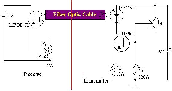
2) Connect the fiber from the LED to the optical power meter.
3) Adjust R1 so that the voltage at the emitter is 4V.
4) Measure the voltage across the LED.
5) Measure the optical power from the LED.
6) Calculate the current through the LED.
7) Repeat steps 4 through 6 for emitter voltages of 3.7V, 3.4V, 3.1V, 2.8V, 2.5V, 2.2V, 1.9V, 1.6V, 1.3V, 1.0V, .7V, .4V, and .1V.
8) Connect the fiber optic cable to the remote side.
9) Set the emitter voltage back to 4V.
10) Adjust RL so that the voltage across it is at least 2V.
11) Measure the voltage across RL.
12) Calculate the current through RL.
13) Repeat steps 11 and 12 for emitter voltages of 3.7V, 3.4V, 3.1V, 2.8V, 2.5V, 2.2V, 1.9V, 1.6V, 1.3V, 1.0V, .7V, .4V, and .1V.
B: Analog Optical Communications
1) Assemble the following
circuit:
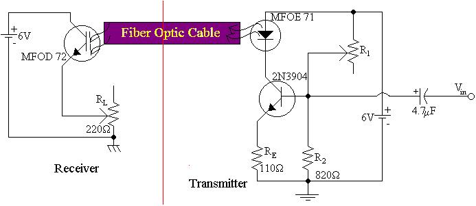
2) Power the detector circuit.
4) Measure, and calculate the current through RL, the dark current.
5) Remove power from the detector and power the transmitter side.
6) Saturate the transistor to allow the diode to emit maximum power.
7) Calculate the current through the LED assuming a voltage drop of 1.5V.
8) Calculate the power dissipated by RE, determine if it is beyond the rated power dissipation of ½ watt.
9) Calculate the minimum resistor value necessary to meet the ½ watt specification and determine if that value will allow saturation of the LED.
10) Power both the receiver and transmitter.
11) Adjust R1 so the current through the LED is between 10ma and 15ma.
12) Apply a 1Vpp, 1KHz sine wave to the input of the transmitter.
13) Observe the output of the receiver to ensure that it is an optimized sine wave, adjust RL if it is not.
14) Using the gain – phase meter, observe the signal loss through the link.
15) Repeat step 14 using sine waves of 2KHz, 5KHz, 10KHz, 20KHz, 50KHz, 100KHz, 200KHz, and 500KHz.
16) Make additional measurements to find the -3dB point as necessary.
17) Repeat steps 14 through 16 using double RL, triple RL, and quadruple RL.
C: Digital Optical Communications
1) Assemble the following
circuit:
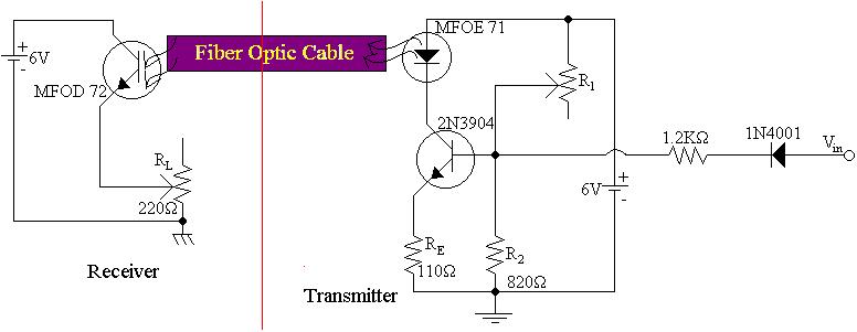
2) Starting with RL of approximately 500W, and using a decade box to set R1 to 20KW, power the transmitter to 2V.
3) Power the receiver and adjust RL until the voltage across it is 3V.
4) Find the lowest transmitter voltage that produces a voltage drop across RL.
5) Set the transmitter voltage to 4V.
6) Record voltage across R1, base voltage, voltage across Rc, the voltage across the LED, and the voltage across RL.
7) Calculate the current through the decade box, the 820W resistor, base current, collector current, and current through RL.
8) Repeat step 6 and 7 for transmitter voltages of 3.5V, 3V, 2.5V, 2V, 1.5V, 1V, and .5V.
9) Remove the decade box from the circuit and connect the function generator.
10) Set the function generator to generate a 1KHz 4Vpp square wave.
11) Ensure that there is a signal visible across the load resistor, if not, increase the function generator's output voltage.
12) Measure the rise and fall time for the circuit.
13) Calculate the bit rate of the circuit.
14) Measure the average base voltage, the voltage across Rc, and the voltage across the LED.
15) Measure the voltage across RL.
16) Repeat steps 13 through 15 for frequencies of 1KHz, 2KHz, 4KHz, 8KHz, 16KHz, 32KHz, 64KHz, and 128KHz.
17) Using a double RL, triple RL and quadruple RL, repeat the RL measurement for the frequencies given in step 16.
![]() Lab
Data / Results
Lab
Data / Results
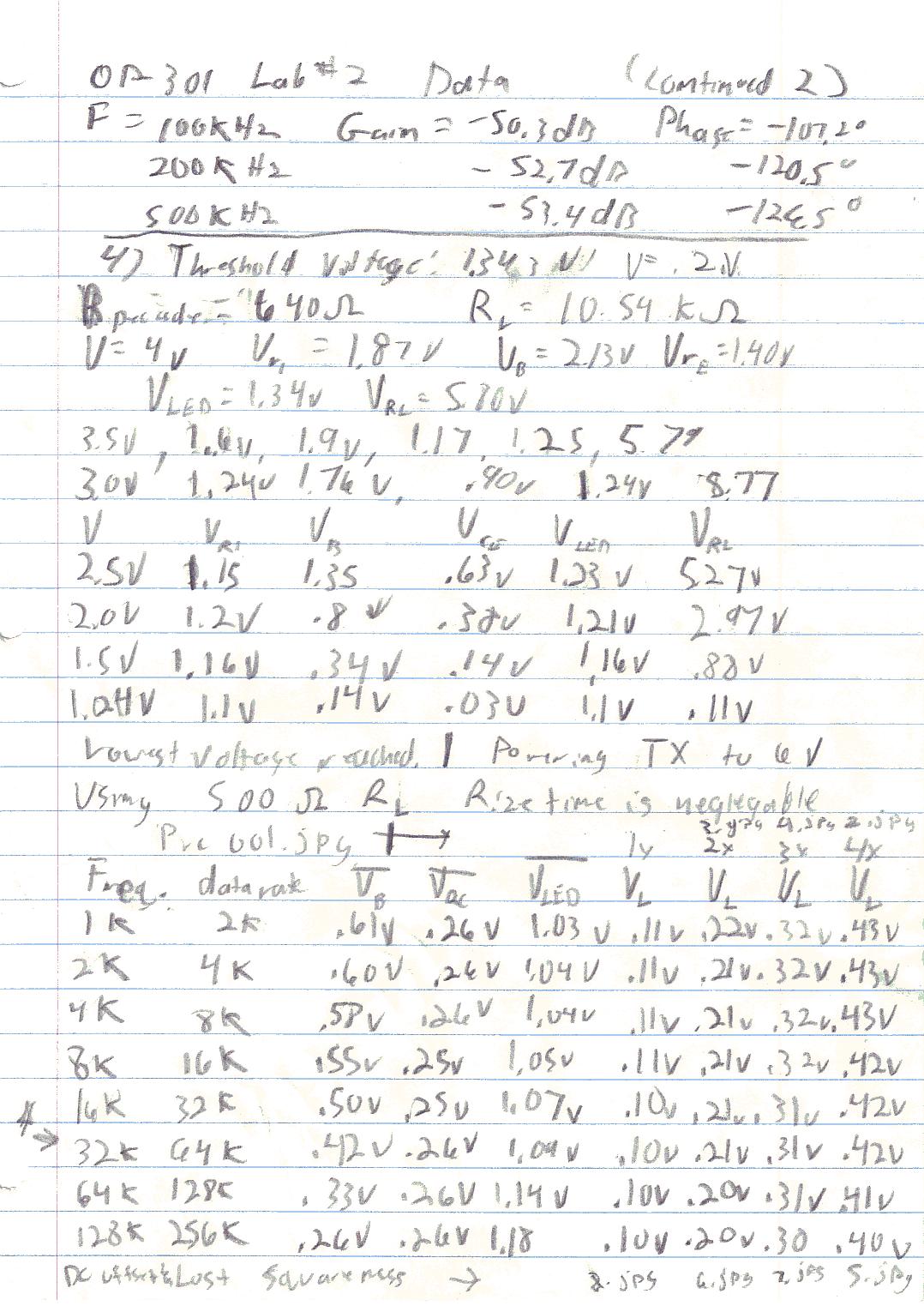
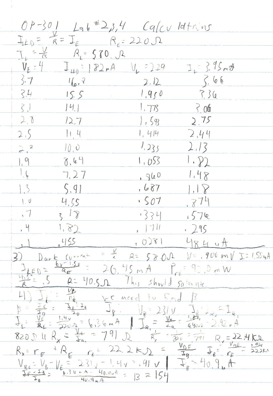
1) Table 1: Transmitter Threshold
|
R1 |
RL |
Threshold Voltage: |
Load Voltage: |
|---|---|---|---|
|
640W |
10.54KW |
1.343V |
.2V |
2) Diagram 1: Schematic 1 enlarged view

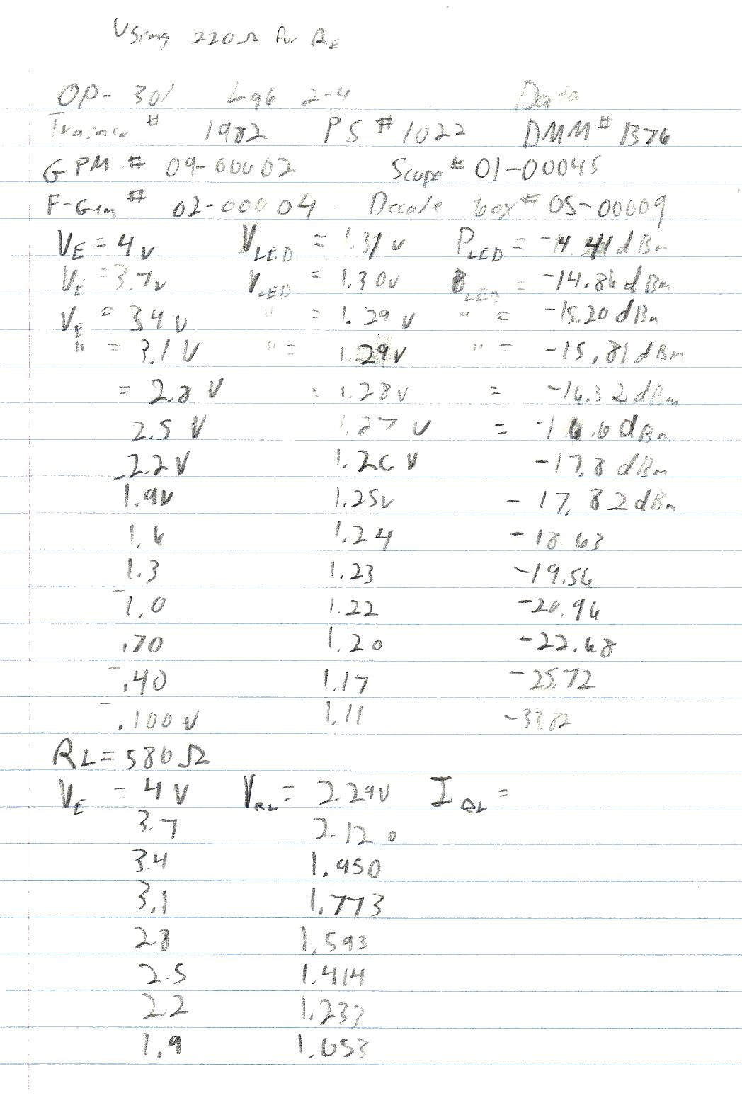
3) Table 2: LED Power vs. Optical Power vs. Receiver Current:
|
VE |
VLED |
Optical Power |
LED Current |
Load Voltage |
Load Current |
|---|---|---|---|---|---|
|
4.0V |
1.31V |
-14.41dBm |
18.2mA |
2.29V |
3.95mA |
|
3.7V |
1.30V |
-14.86dBm |
16.8mA |
2.12V |
3.66mA |
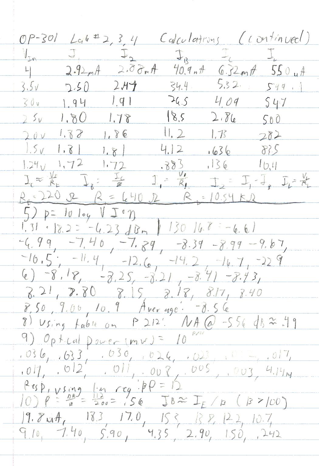
|
3.4V |
1.29V |
-15.20dBm |
15.5mA |
1.950V |
3.36mA |
|
3.1V |
1.29V |
-15.81dBm |
14.1mA |
1.773V |
3.06mA |
|
2.8V |
1.28V |
-16.32dBm |
12.7mA |
1.593V |
2.75mA |
|
2.5V |
1.27V |
-16.60dBm |
11.4mA |
1.414V |
2.44mA |
|
2.2V |
1.26V |
-17.80dBm |
10.0mA |
1.233V |
2.13mA |
|
1.9V |
1.25V |
-17.82dBm |
8.64mA |
1.053V |
1.82mA |
|
1.6V |
1.24V |
-18.63dBm |
7.27mA |
.860V |
1.48mA |
|
1.3V |
1.23V |
-19.56dBm |
5.91mA |
.687V |
1.18mA |
|
1.0V |
1.22V |
-20.96dBm |
4.55mA |
.507V |
0.87mA |
|
.70V |
1.20V |
-22.68dBm |
3.18mA |
.334V |
0.58mA |
|
.40V |
1.17V |
-25.72dBm |
1.82mA |
.1711V |
0.30mA |
|
.10V |
1.11V |
-33.82dBm |
0.46mA |
.0281V |
48.4mA |
4) Diagram 2: Schematic 2 enlarged view:

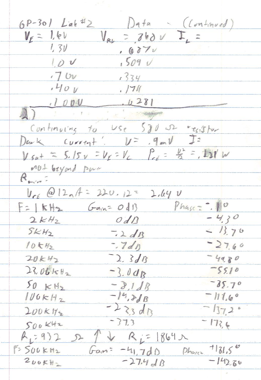
5) Table 3: Saturation Voltage:
|
Voltage: |
Current: |
Resistance: |
Power: |
Will it Saturate? |
|---|---|---|---|---|
|
1.5 |
20.45mA |
220W |
92.0mW |
No |
|
1.5 |
333mA |
40.5W |
500mW |
Yes |
|
.85V |
142mA |
220W |
121mW |
Yes |
6) Table 4: Gain - Phase Observations using RL = 932W
|
Frequency |
Gain |
Phase |
|---|---|---|
|
1KHz |
0dB |
-0.1o |
|
2KHz |
0dB |
-4.3o |
|
5KHz |
-0.2dB |
-13.7o |
|
10KHz |
-0.7dB |
-27.6o |
|
20KHz |
-2.3dB |
-49.8o |
|
23.06KHz |
-3.0dB |
-55.1o |
|
50KHz |
-8.1dB |
-85.7o |
|
100KHz |
-14.8dB |
-111.6o |
|
200KHz |
-22.3dB |
-137.2o |
|
500KHz |
-37.3dB |
-173.6o |
7) Table 5: Dark Current:
|
Dark Voltage: |
Dark Current: |
|---|---|
|
.9mV |
1.55mA |
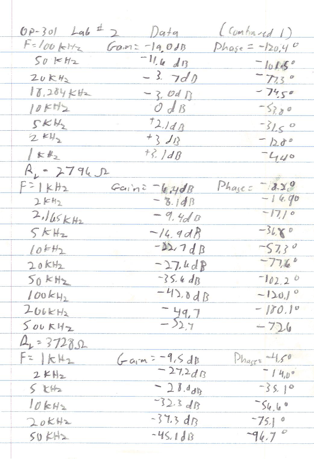
8) Table 6: Gain - Phase Observations using RL = 1864W
|
Frequency |
Gain |
Phase |
|---|---|---|
|
1KHz |
+3.1dB |
-4.4o |
|
2KHz |
+3dB |
-12.8o |
|
5KHz |
+2.1dB |
-31.5o |
|
10KHz |
0dB |
-53.8o |
|
18.284KHz |
-3.0dB |
-74.5o |
|
20KHz |
-3.7dB |
-77.3o |
|
50KHz |
-11.6dB |
-101.5o |
|
100KHz |
-19.0dB |
-120.4o |
|
200KHz |
-27.4dB |
-142.8o |
|
500KHz |
-41.7dB |
+181.5o |
9) Table 7: Gain - Phase Observations using RL = 2796W
|
Frequency |
Gain |
Phase |
|---|---|---|
|
1KHz |
-6.4dB |
-8.2o |
|
2KHz |
-8.1dB |
-16.9o |
|
2.165KHz |
-9.4dB |
-17.1o |
|
5KHz |
-16.9dB |
-13.8o |
|
10KHz |
-22.7dB |
-57.3o |
|
20KHz |
-27.6dB |
-77.6o |
|
50KHz |
-35.6dB |
-102.2o |
|
100KHz |
-42.8dB |
-120.1o |
|
200KHz |
-49.7dB |
-180.1o |
|
500KHz |
-52.7dB |
-72.6o |
10) Table 8: Gain - Phase Observations using RL = 3728W
|
Frequency |
Gain |
Phase |
|---|---|---|
|
1KHz |
-9.5dB |
-4.5o |
|
2KHz |
-27.2dB |
-14.0o |
|
5KHz |
-28.9dB |
-35.1o |
|
10KHz |
-32.3dB |
-56.6o |
|
20KHz |
-37.3dB |
-75.1o |
|
50KHz |
-45.1dB |
-96.7o |
|
100KHz |
-50.3dB |
-107.2o |
|
200KHz |
-52.7dB |
-120.5o |
|
500KHz |
-53.4dB |
-126.5o |
11) Diagram 3: Schematic 3 enlarged view:

12) Table 9: Transmitter Input Voltage Table (Voltage):
|
Vin |
VR1 |
VB |
VRE |
VLED |
VL |
|---|---|---|---|---|---|
|
4.0V |
1.87V |
2.13V |
1.40V |
1.34V |
5.80V |
|
3.5V |
1.60V |
1.90V |
1.17V |
1.25V |
5.79V |
|
3.0V |
1.24V |
1.76V |
.90V |
1.24V |
5.77V |
|
2.5V |
1.15V |
1.35V |
.63V |
1.23V |
5.27V |
|
2.0V |
1.2V |
.80V |
.38V |
1.21V |
2.97V |
|
1.5V |
1.16V |
.34V |
.14V |
1.16V |
.88V |
|
1.24V |
1.1V |
.14V |
.03V |
1.1V |
.11V |
13) Table 10: Transmitter Input Voltage Table (Current):
|
Vin |
I1 |
I2 |
IB |
IC |
IL |
|---|---|---|---|---|---|
|
4.0V |
2.92mA |
2.88mA |
40.9mA |
6.32mA |
550mA |
|
3.5V |
2.50mA |
2.47mA |
34.4mA |
5.32mA |
549mA |
|
3.0V |
1.94mA |
1.91mA |
26.5mA |
4.09mA |
547mA |
|
2.5V |
1.80mA |
1.78mA |
18.5mA |
2.86mA |
500mA |
|
2.0V |
1.88mA |
1.86mA |
11.2mA |
1.73mA |
282mA |
|
1.5V |
1.81mA |
1.81mA |
4.12mA |
.636mA |
83.5mA |
|
1.24V |
1.72mA |
1.72mA |
.883mA |
.136mA |
10.4mA |
14) Table 11: Average Voltages for Digital Transmission:
|
Frequency: |
Data Rate: |
VB |
VRC |
VLED |
VL |
2*VL |
3*VL |
4*VL |
|---|---|---|---|---|---|---|---|---|
|
1KHz |
2Kbps |
.61V |
.26V |
1.03V |
.11V |
.22V |
.32V |
.43V |
|
2KHz |
4Kbps |
.60V |
.26V |
1.04V |
.11V |
.21V |
.32V |
.43V |
|
4KHz |
8Kbps |
.58V |
.26V |
1.04V |
.11V |
.21V |
.32V |
.43V |
|
8KHz |
16Kbps |
.55V |
.25V |
1.05V |
.11V |
.21V |
.32V |
.42V |
|
16KHz |
32Kbps |
.50V |
.25V |
1.07V |
.10V |
.21V |
.31V |
.42V |
|
32KHz |
64Kbps |
.42V |
.26V |
1.09V |
.10V |
.21V |
.31V |
.42V |
|
64KHz |
128Kbps |
.33V |
.26V |
1.14V |
.10V |
.20V |
.31V |
.41V |
|
128KHz |
256Kbps |
.26V |
.26V |
1.18V |
.10V |
.20V |
.30V |
.40V |
15) Table 12: Rise Time for signals
|
Load Resistor: |
1.0KW |
1.5KW |
2KW |
500W |
|---|---|---|---|---|
|
Rise Time: |
negligible |
negligible |
negligible |
negligible |
16) Diagram 4: Rise time signal for RL = 500W
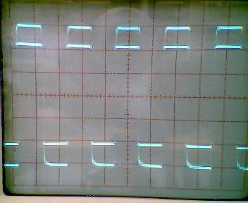
17) Diagram 5: Rise time signal for RL = 1KW
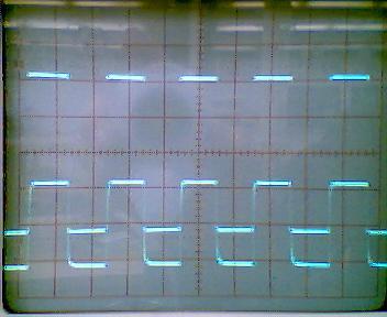
18) Diagram 6: Rise time signal for RL = 1.5KW
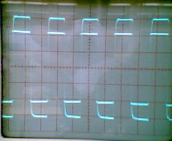
19) Diagram 7: Rise time signal for RL = 2KW
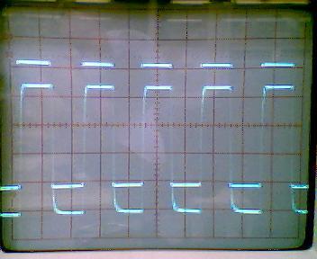
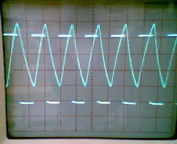
20) Diagram 8: Maximum Data Rate signal for RL = 500W
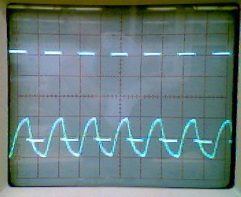
21) Diagram 9: Maximum Data Rate signal for RL = 1KW
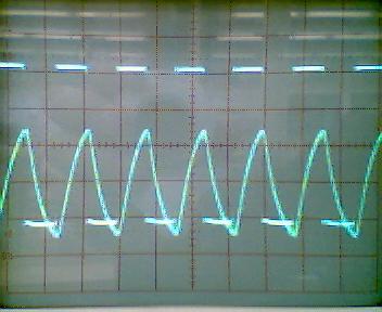
22) Diagram 10: Maximum Data Rate signal for RL = 1.5KW
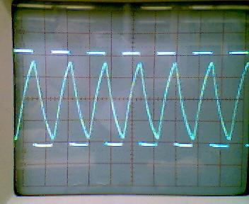
23) Diagram 11: Maximum Data Rate signal for RL = 2KW
![]() Answers to Lab Question
Answers to Lab Question
1) Q: What wavelength does the LED emit?
A: 1310nM
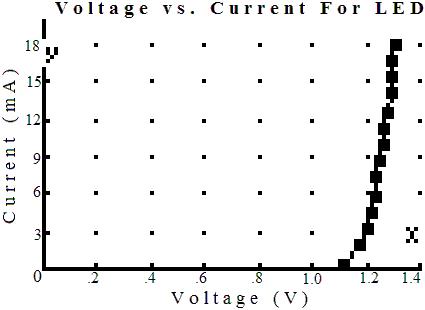
2) Q: Plot ID vs. VD for the LED, what is the turn-on voltage?.
A: About 1.1V
3) Q: Using the answer to Q1, what material is the LED made of?
A: InGaAs
4) Q: Plot the LED's optical power vs. forward current.
A: 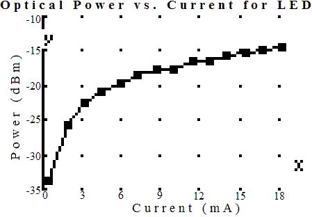
5) Q: Using an assumed efficiency of 1%, calculate and plot the expected optical power output of the LED, and overlay it with the existing plot.
A: 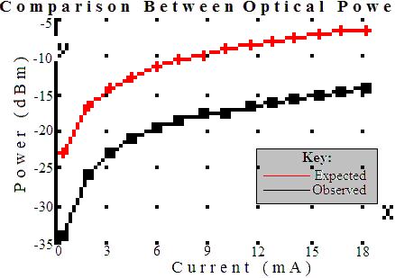
6) Q: Calculate the difference, in dB, for the data in Q5.
A: Power Output
|
Observed: |
Expected: |
Difference: |
|---|---|---|
|
-14.41dBm |
-6.23dBm |
-8.18dB |
|
-14.86dBm |
-6.61dBm |
-8.25dB |
|
-15.20dBm |
-6.99dBm |
-8.21dB |
|
-15.81dBm |
-7.40dBm |
-8.41dB |
|
-16.32dBm |
-7.89dBm |
-8.43dB |
|
-16.60dBm |
-8.83dBm |
-8.21dB |
|
-17.80dBm |
-9.00dBm |
-8.80dB |
|
-17.82dBm |
-9.67dBm |
-8.15dB |
|
-18.63dBm |
-10.5dBm |
-8.18dB |
|
-19.56dBm |
-11.4dBm |
-8.17dB |
|
-20.96dBm |
-12.6dBm |
-8.40dB |
|
-22.68dBm |
-14.2dBm |
-8.50dB |
|
-25.72dBm |
-16.7dBm |
-9.00dB |
|
-33.82dBm |
-22.9dBm |
-10.9dB |
|
Average: |
|
-8.56dB |
7) Q: Assuming a 3dB connection loss, what, then, is the coupling loss of the system?
A: -5.56dB
8) Q: Assuming the LED is a Lambertain source, what is the NA of the fiber?
A: NA Z .49
9) Q: Plot the optical power vs. the load current, what is the responsivity of the detector?
A: br Z 112
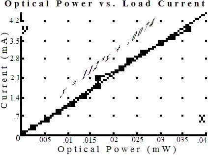
10) Q: Assuming the phototransistor has a b of 200, calculate r for the base of the transistor, and show the base current for Table 2.
A: r Z .56
Power is in dB Current is in mA
|
Pi |
-14.4 |
-14.9 |
-15.2 |
-15.8 |
-16.3 |
-16.6 |
-17.8 |
-17.8 |
-18.6 |
-19.6 |
-21.0 |
-22.7 |
-25.7 |
-33.8 |
|---|---|---|---|---|---|---|---|---|---|---|---|---|---|---|
|
IB |
19.8 |
18.3 |
17.0 |
15.3 |
13.8 |
12.2 |
10.7 |
9.10 |
7.40 |
5.90 |
4.35 |
2.90 |
1.50 |
.242 |
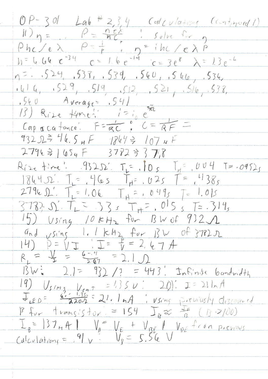
11) Q: Calculate the quantum efficiency of the photodiode.
A: h Z .541
12) Q: Plot the transfer function for all four values of RL.
A:
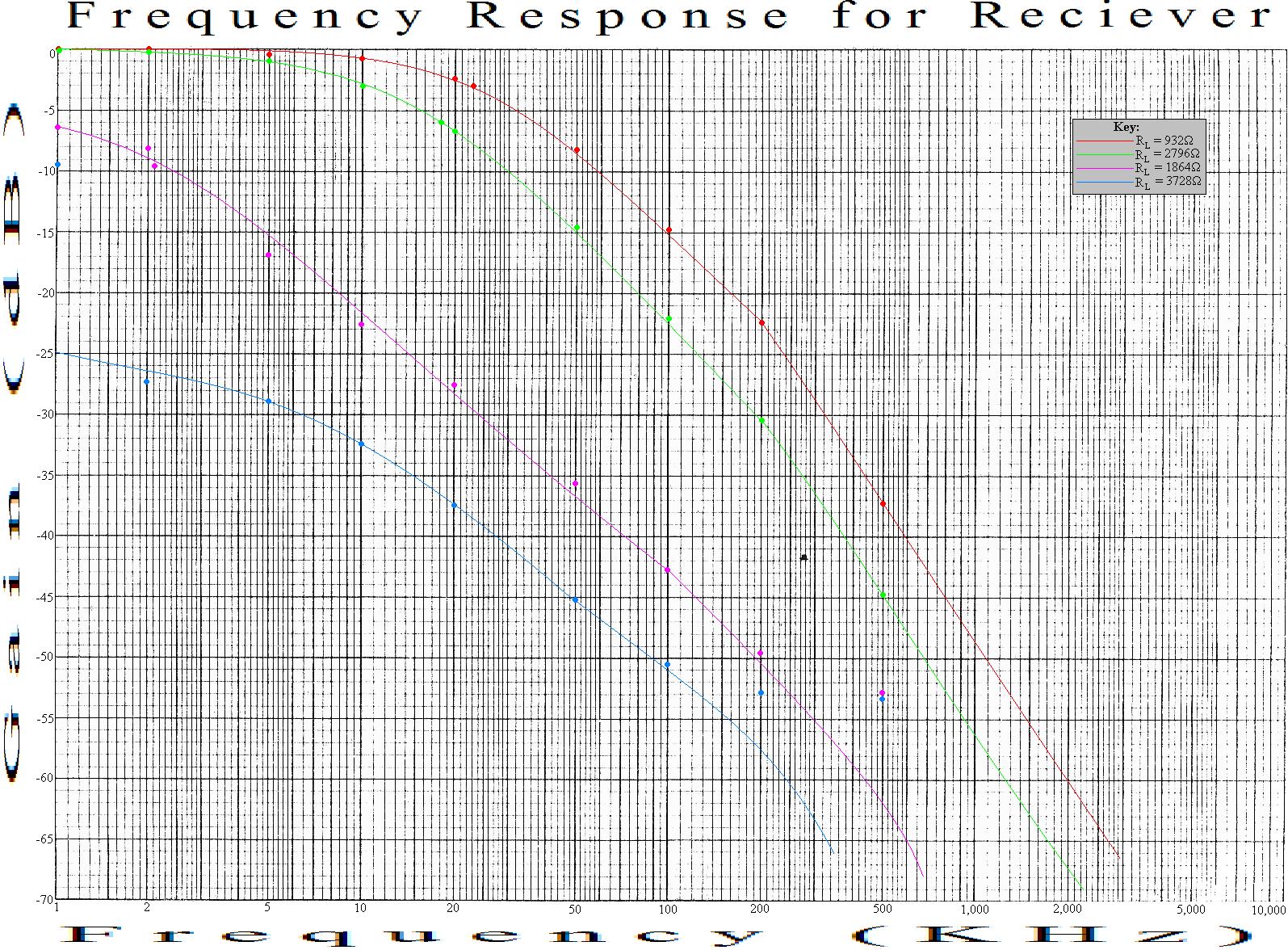
13) Q: Using the -3dB point, calculate the capacitance of the photodetector, and the rise time, also show the phase.
A: Average Capacitance: 89.1mF
|
Resistance: |
932W |
1864W |
2796W |
3782W |
|---|---|---|---|---|
|
-3dB Point: |
23.06KHz |
5.01KHz |
2.165KHz |
7KHz |
|
Capacitance: |
46.5mF |
107mF |
165mF |
37.8mF |
|
Phase Angle: |
-55.1o |
-74.5o |
-17.1o |
-45.9o |
|
Rise-Time |
.0952s |
.438s |
1.01s |
.314s |
14) Q: If the saturation voltage of the phototransistor is .4V and the maximum power dissipation is 150mW, what is the maximum load current, and minimum RL? What, then would be the maximum bandwidth?
A: IL = 2.67A; RL = 2.1W; Infinite bandwidth
15) Q: Plot RL vs. the -3dB bandwidth. What would the bandwidth be for RL = 1KHz? Also, plot the peak output voltage.
A: BW Z 9.5KHz
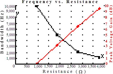
16) Q: What would be the optimal load resistance?
A: Optimal Resistance: 2.2KW
17) Q: What would be the expected output voltage , relative to input voltage, and bandwidth for the resistance selected in Q16?
A: Gain : 4dB Bandwidth: 4KHz
18) Q: What is the minimum transmitter voltage that will produce an output signal?
A: 1.343V
19) Q: What voltage would be required at the input of schematic 3 to saturate the LED?
A: Vsat = 5.56V
20) Q: When the LED is saturated by this voltage, how much current flows through it?
A: ILED = 21.1mA
21) Q: What is the b of the transistor?
A: b = 154
22) Q: What are the rise and fall times for each RL?
A: Rise and fall times were negligible, and scope was not able to illustrate them.
23) Q: Based on the rise time estimates, what is the capacitance of the photodiode?
A: Insufficient data to perform calculation. Capacitance is < 100nF.
24) Q: How does this capacitance compare to the one discovered in Q13?
A: The capacitances are totally different.
25) Q: What correlation, if any, exist between the bandwidth and the rise time?
A: There is no correlation because the bandwidth is more determined on the ability for the system to hold the voltage for sampling more than transition time.
26) Q: What is the maximum NRZ for each load resistor?
A:
|
Resistance: |
500W |
1KW |
1.5KW |
2KW |
|---|---|---|---|---|
|
Maximum Data Rate: |
64Kbps |
64Kbps |
64Kbps |
64Kbps |
27) Q: If 1V were required at the load, what would be the maximum NRZ data rate for the system?
A: 64Kbps
![]() Conclusions
Conclusions
This lab has demonstrated the basic principles surrounding a basic fiber-optic communications system. However, this system does not accurately model the actual world. The equipment used was horrible out of calibration and there were many difficulties associated with the lab. Primarily a 220W resistor was substituted for the 110W resistor in the schematics. Although the direct impact on the lab was mostly easily compensated for, it could explain some of the radical errors observed in the data sets. The analog measurements have little to no foundation and were not reproducible. The reason for this is as of yet, undiscovered. The system, overall exhibited a high level of loss, uncharacteristic of a fiber-optic system. Much of the loss is most likely as a direct result of equipment being out of calibration. This may explain the radical readings observed in the analog section. The analog section suggested two possible data sets. One involving the 3.7KW and 930W load resistance, and one involving the 1.7KW and 2.7KW load resistance. There is insufficient data to support or disprove either of these two systems. As a result, calculations were made in sets to show the most accurate representation of the data possible. The digital system represented a much more accurate set of readings. However, the maximum data rate calculation is uncertain. The observation was made based on the requirement of a PECL quantizer being placed at the receive end which requires only a rise-and-hold time to determine a 1 or 0 state. For this, 1% of the wave time was used. Additionally, since the low output resistance was used, the rise and fall times were unable to be read. On the oscilloscope they appeared as a perfect straight line. However, it would have been possible to make a more accurate measurement had the time base been properly adjusted. Unfortunately, this was overlooked. Also, the lab handout schematic calls out a 220W resistor to be placed in series with the LED. This was omitted to have a higher power output and to be compatible with other readings. It was also omitted to help compensate for the increase in emitter resistance. As a result, RE voltage was read in lieu of RC. It would be interesting to see if the capacitive effect of the photodiode could be reduced if the phototransistor was arranged in a common-collector or Darlington configuration as opposed to a common emitter.
![]() Attachments
Attachments
