![]() Objective
Objective
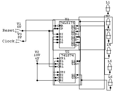
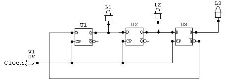
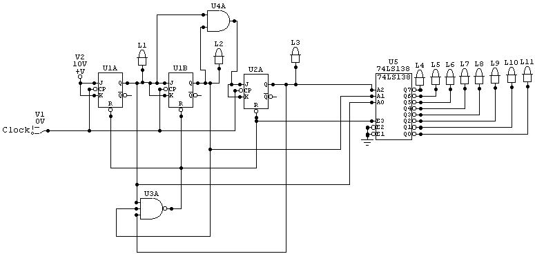
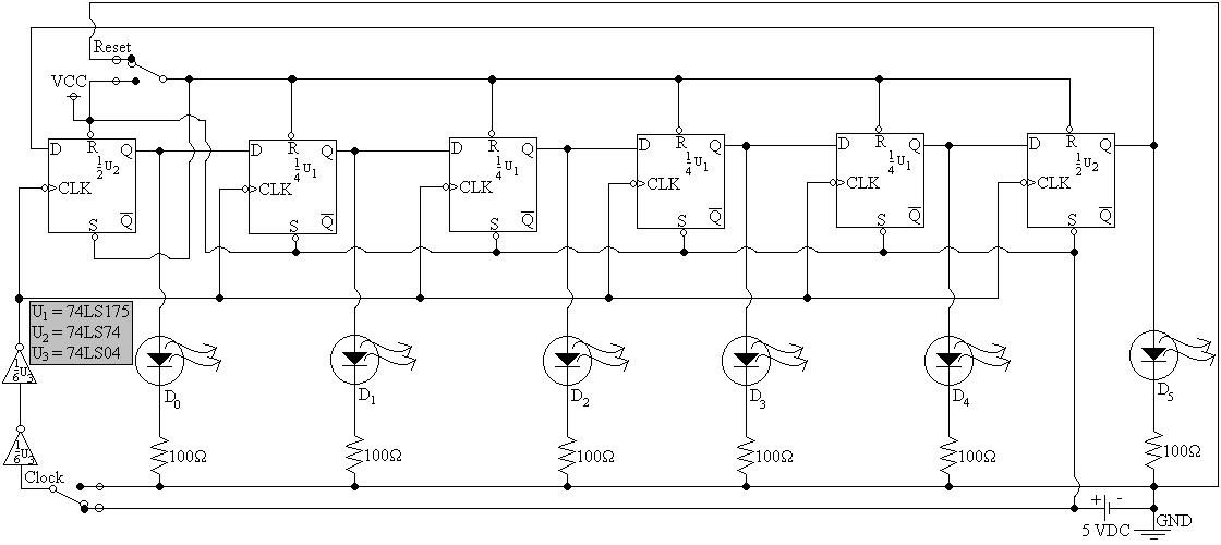
The objective of this lab is to construct, through simulation, several types of 6 state T-State generators using different techniques. Then to use those designs to evaluate the advantages and disadvantages of each different type. Then to construct and test the operation of one of the state generators to justify the design choice.
![]() Components Used
Components Used
1) Computer with Logic Aid ® , and Circuit Maker ® software Packages.
2) Digital Trainer #1060
3) D Type Flip-Flips (6)
4) Various components of the EE - 304 lab kit
![]() Procedures
Procedures
1) Design and test the output of a ring counter using D Flip-Flops.
2) Design and test the same counter using J-K Flip-Flops.
3) Design a Johnson counter and test the counter.
4) Create a MSI counter to Decoder and test the operation.
5) Physically construct and test the operation of a D Flip-Flop ring counter, and test operation.
![]() Lab Data /Results
Lab Data /Results
1) Diagram 1: D - Type Flip - Flop Ring Counter Design

2) Diagram
2: J - K Type Flop - Flop Ring Counter Design

3) Diagram 3: Johnson Counter Design

4) Diagram 4: MSI Counter With Decoder Design

5) Table 1: Results from In - Lab Experiment
|
|
D0 |
D1 |
D2 |
D3 |
D4 |
D5 |
|---|---|---|---|---|---|---|
|
Initial: |
1 |
0 |
0 |
0 |
0 |
0 |
|
State 2: |
0 |
1 |
0 |
0 |
0 |
0 |
|
State 3: |
0 |
0 |
1 |
0 |
0 |
0 |
|
State 4: |
0 |
0 |
0 |
1 |
0 |
0 |
|
State 5: |
0 |
0 |
0 |
0 |
1 |
0 |
|
State 6: |
0 |
0 |
0 |
0 |
0 |
1 |
|
State 7: |
Return to Initial State |
|||||
6) Diagram 5: Schematic of Assembled Ring Counter

![]() Conclusions
Conclusions
This lab has demonstrated the construction of three different types of state generators. Also, it has demonstrated multiple ways of constructing each. Additionally, using the D - Type Flip - Flop, it has demonstrated that these generators can be easily realized with few, if any, changes that need to be made to the simulated schematic to realize the function. In testing, i found that the circuit, with the input buffer on the clock, is very stable, even at high frequencies ( > 1MHz). I also tested the effects of an offset DC signal at the clock input. I found the system to be quite intolerant of a significant DC offset. It also had a good clock voltage range (2.4V - 6V approximately). I took many different reading with the realized circuit to ensure that it was operating properly and am pleased with the results. For the complete set of readings taken, please see the attachments.
![]() Attachments
Attachments