![]() Objective
Objective
The objective of this lab is to illustrate gate reduction through several means, including commercially available LogicAid ® and the use of Quine-McClusky reduction. Ultimately obtaining a lowest gate set comprising only of NAND gates and 1 inverter chip. Then to test the final results to see if the correct truth table is created. Lastly, to re-implement the same circuit using NOR gates.
![]() Components Used
Components Used
1) Computer With LogicAid ©, and CircuitMaker ©
![]() Procedures
Procedures
1) Using Quine-McClusky methods, simplify the following Boolean function to consist of only NAND gates and an inverter: f(abcdefg) = S(4, 5, 6, 7, 14, 16, 17, 18, 20, 21, 22, 23, 24, 25, 26, 28, 29, 30, 36, 37, 38, 39, 42, 46, 48, 49, 50, 52, 53, 54, 55, 56, 57, 60, 61, 66, 68, 69, 70, 71, 74, 78, 82, 84, 85, 86, 87, 90, 94, 98, 101, 102, 103, 106, 110, 114, 117, 118, 119) + d(2, 10, 34)
2) Using various techniques, simplify the system to use as few chips as possible.
3) Simulate the circuit on CircuitMaker.
4) Derive a a NOR-gate implementation of the same circuit.
5) Simulate that circuit on CircuitMaker.
![]() Lab Data / Results
Lab Data / Results
1) Data 1: Output from LogicAid ®:
_ _ _ _ _ _ _ _ _ _ _ _ _
X = DEG + FDG + CFG + BFG + BDE + ACF + ADE
2) Data 2: Reduced for Minimal Chip Count:
_ _ _ _ _ _ _ _ _
X = (A + B + G)DE + (B + C + D)FG + ACF
3) Data 3: Results from Quine - McCluskey Tabulation:
__ __ __ __ __ __ __ __ __ __ __ __ __ __ __ __ __
X = ACDF G + ACDF + BFG + CFG + ADE + BDE + ACG + DEG
4) Data 4: NOR Gate Implementation form LogicAid ®:
_ _ _ _ _ _ _ _ _ _ _
X = (A + B + F + G) * (A + D + F) * (A + E + F) * (B + C + D + F) * (E + F + G)
__ __ __ __
(C + D + F) * (D + F + G) * (C + E + F)
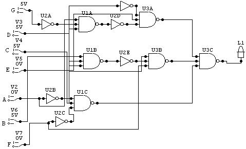
5) Diagram 1: LogicAid ® NAND Gate Implementation:

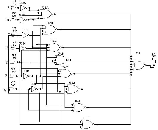
6) Diagram 2: LogicAid ® NOR Gate Implementation:

![]() Conclusions
Conclusions
From this lab it is proven that the given function can be implemented with only three logic chips: 2 - 7410s and 1 7404 chip. Additionally this function can be reproduced using NOR logic with at most 1 7400 HEX inverter, 1 dual 4 - input NOR chip , 2 triple 3 - input NOR gates, and 1 8 - input NOR gate. I would like to note that I did manually perform the Quine - McCluskey Tabulation, and while however did not come up with the same results as LocigAid ® did, I was satisfied with my results. The primary reason for the discrepancy was a tabulation error. I forgot to include the value 118 in the tabulation and therefore the value was not taken into consideration for subsequent logic reductions. Additionally, the massive amount of data that was involved in the algorithm caused a degree of human error over the 28+ hours of work that were involved in performing the operation. Overall I believe that this lab was successful. As an extra, I used LogicAid to run a reduction omitting the value 118 from the simplification. Unfortunately the results did not resemble in any way the results I received from my tabulation. The results are as follows:
__ __ __ __ __ __ __ __ __ __ __ __ __ __
X = DEG + DEFG + CFG + BFG + BDE + ACF + ADE
![]() Attachments
Attachments