![]() Objective
Objective
EL - 204
Digital Electronics
Lab #4 Implementation of Logic Networks
Andrew Buettner
![]() Objective
Objective
The objective of this lab is to combine gates, a truth table, and a data selector to implement a typical logic function.
![]() Equipment Used
Equipment Used
1) Logic Trainer #00505016
2) 7408 two input AND gate
3) 7432 two input OR gate
4) 74151A data selector
5) Logic probe
6) Logic pulser
![]() Procedure
Procedure
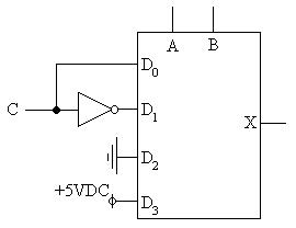
1)
Assemble the following circuit:
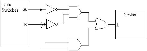
2) Create a truth table to describe the circuit's operation
3)
Assemble the following circuit:
4) With Switch A set to 0 note the effects of switching D0 and D1
5) Set Switch A to 1 and observe the new effects
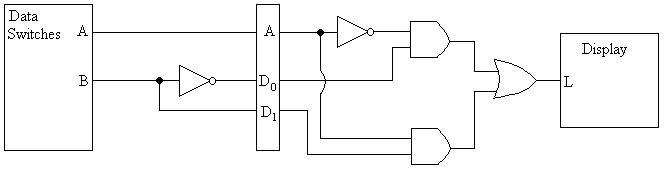
6) Create a circuit using the previous circuit that will have the following truth table:
|
A |
B |
C |
|---|---|---|
|
0 |
0 |
1 |
|
0 |
1 |
0 |
|
1 |
0 |
0 |
|
1 |
1 |
1 |
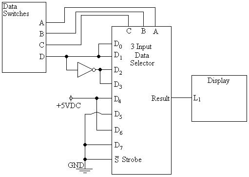
7) Assemble a circuit using the three bit data selector that will be used in a football
game to do the following:
i) Have two players, offense and defense
ii) Each player has two options: Run / Pass and Left / Right
iii) The players select their play then an output LED displays if the play was successful or not
iv) The logic of the game should work as follows:
a) If the offense selects pass, and the defense selects run the play works no matter what
direction wither choose
b) If the offense chooses run, and the selected directions are opposite, the play is successful
no matter what the defense chooses
c) All other combinations result in a failure
8) Create a truth table showing the results of the circuit
![]() Data / Results
Data / Results
1) Table 1: Truth Table for Schematic #1
|
A |
B |
C |
|---|---|---|
|
0 |
0 |
1 |
|
0 |
1 |
0 |
|
1 |
0 |
0 |
|
1 |
1 |
1 |
2) Diagram 1: Schematic #1, Enlarged View

3) Table 2: Truth Table Describing Schematic #2
|
A |
D0 |
D1 |
X |
|---|---|---|---|
|
0 |
0 |
0 |
0 |
|
0 |
0 |
1 |
0 |
|
0 |
1 |
0 |
1 |
|
0 |
1 |
1 |
1 |
|
1 |
0 |
0 |
0 |
|
1 |
0 |
1 |
1 |
|
1 |
1 |
0 |
0 |
|
1 |
1 |
1 |
1 |
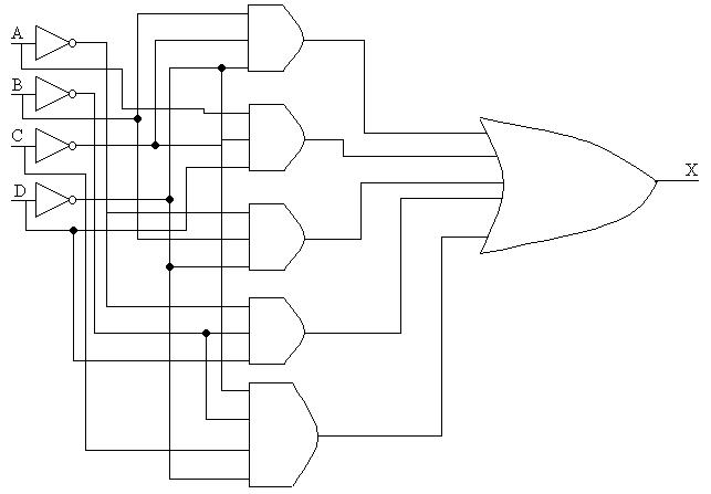
4) Diagram 2: Schematic solution for procedure 7
5) Table 3: Truth Table for Schematic Featured in Diagram 4
|
A |
B |
C |
D |
X |
|---|---|---|---|---|
|
0 |
0 |
0 |
0 |
0 |
|
0 |
0 |
0 |
1 |
1 |
|
0 |
0 |
1 |
0 |
0 |
|
0 |
0 |
1 |
1 |
1 |
|
0 |
1 |
0 |
0 |
1 |
|
0 |
1 |
0 |
1 |
0 |
|
0 |
1 |
1 |
0 |
1 |
|
0 |
1 |
1 |
1 |
0 |
|
1 |
0 |
0 |
0 |
1 |
|
1 |
0 |
0 |
1 |
1 |
|
1 |
0 |
1 |
0 |
0 |
|
1 |
0 |
1 |
1 |
0 |
|
1 |
1 |
0 |
0 |
1 |
|
1 |
1 |
0 |
1 |
1 |
|
1 |
1 |
1 |
0 |
0 |
|
1 |
1 |
1 |
1 |
0 |
6) Diagram 2: Schematic #2, Enlarged View

7) Diagram 3: Schematic Solution for procedure 6
![]() Answers To Lab Questions
Answers To Lab Questions
1) Q: If there were no output from the data selector no matter what the inputs were, even if they were correct, what check should be made first?
A: The voltage at the strobe, it should be low.
2) Q: What
is the Boolean expression for the following circuit?
_ _ _
A: AB + BC + ABC
3) Q: What are the advantages of using two eight input data selectors or one sixteen input data selector to implement a five variable expression?
A: The advantage of using eight input data selectors is that the connections would be easier to make because there would be less pins, while the advantage of using a sixteen input data selector is that the circuit would be smaller and consume less power because there are fewer components.
4) Q: Draw a mechanical switch equivalent for a four input data selector
A: 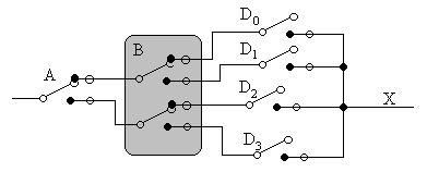
5) Q: Create a Karnaugh map and circuit using conventional gates to replicate the football game.
A:
|
|
C=0 D=0 |
C=0 D=1 |
C=1 D=1 |
C=1 D=0 |
|---|---|---|---|---|
|
A=0 B=0 |
|
1 |
1 |
|
|
A=0 B=1 |
1 |
|
|
1 |
|
A=1 B=1 |
1 |
1 |
|
|
|
A=1 B=0 |
|
1 |
|
1 |
6) Q: What is another name for the data selector?
A: PLD / Programmable Logic Device
7) Q: When troubleshooting a data selector the D0, and D4 inputs yield the same results. As do D1 and D5, D2, and D6, and D3 and D7, what selector input is at fault?
A: In this situation, the C input, or MSB is at fault.
![]() Conclusions
Conclusions
From this lab one can conclude that multiple complex logic functions can be easily implemented with the use of a data selector or a Programmable Logic Device.
![]() Attachments
Attachments
1) Original Lab Data
2) Calculations