![]() Objective
Objective
The objective of this lab is to construct a fixed bias circuit using a JFET. Then to use that circuit to determine if a change in the resistor connected to the G connection will affect the operation of the circuit. Then to plot the current flowing through the transistor as a function of voltage.
![]() Equipment Used
Equipment Used
1) Trainer #1278
2) Multimeter #1261
3) 2N4092 N - channel JFET
4) 470W resistor
5) 33KW resistor
6) 1MW resistor
![]() Procedure
Procedure
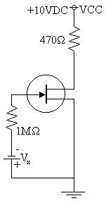
1) Assemble the following circuit:

2) Set VX to be 0V and Measure VDS
3) Calculate ID, IS, and IG using the following values:
a) IDSS = 15mA
b) VP = -6V
4) Repeat steps 2 and 3 using the following voltages:
a) -1V
b) -2V
c) -3V
d) -4V
e) -5V
f) -6V
5) Repeat steps 2 through 4 using a 33KW resistor in place of the 1MW resistor
![]() Data
Data
1) Table 1: Values for 1MW resistor:
|
VX |
VDS |
ID |
IS |
IG |
|---|---|---|---|---|
|
0V |
.517V |
15mA |
15mA |
0mA |
|
-1V |
.639V |
10.4mA |
10.4mA |
0mA |
|
-2V |
.877V |
6.67mA |
6.67mA |
0mA |
|
-3V |
1.936V |
3.75mA |
3.75mA |
0mA |
|
-4V |
7.08V |
1.67mA |
1.67mA |
0mA |
|
-5V |
9.96V |
.417mA |
.417mA |
0mA |
|
-6V |
9.97V |
0mA |
0mA |
0mA |
2) Table 2: Values for 33KW resistor:
|
VX |
VDS |
ID |
IS |
IG |
|---|---|---|---|---|
|
0V |
.477V |
15mA |
15mA |
0mA |
|
-1V |
.636V |
10.4mA |
10.4mA |
0mA |
|
-2V |
.869V |
6.67mA |
6.67mA |
0mA |
|
-3V |
1.935V |
3.75mA |
3.75mA |
0mA |
|
-4V |
7.07V |
1.67mA |
1.67mA |
0mA |
|
-5V |
9.96V |
.417mA |
.417mA |
0mA |
|
-6V |
9.97V |
0mA |
0mA |
0mA |
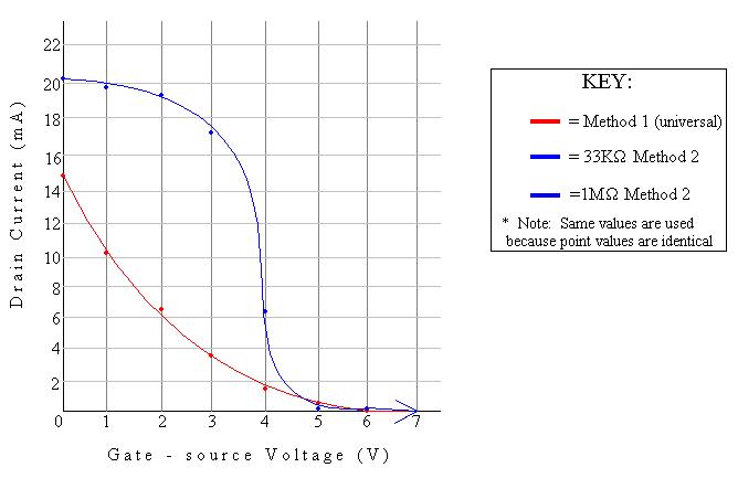
3) Table 3: Comparison of ID through different methods of calculation: * See Conclusions *
R = 1MW R = 33KW
|
VX |
Method 1 |
Method 2 |
Method 1 |
Method 2 |
|---|---|---|---|---|
|
0 |
15mA |
20.2mA |
15mA |
20.3mA |
|
1 |
10.4mA |
19.9mA |
10.4mA |
19.9mA |
|
2 |
6.67mA |
19.4mA |
67mA |
19.4mA |
|
3 |
3.75mA |
17.2mA |
3.75mA |
17.2mA |
|
4 |
1.67mA |
6.21mA |
1.67mA |
6.21mA |
|
5 |
.417mA |
.0851mA |
.417mA |
.0851mA |
|
6 |
0mA |
.0638mA |
0mA |
.0638mA |
3) Diagram 1: Schematic 1, enlarged view:

4) Diagram 2: Graph of VGS vs. ID

![]() Answers to Lab Questions
Answers to Lab Questions
1) Q: Does changing the value of RG have a significant effect on the operation of the circuit and why?
A: No, The Drain - Source voltages are extremely similar between the two data tables, this is expected as IG is always taken to be 0mA causing the resistor to an insignificant component.
2) Q: Is the assumption that VP = -6V a valid one?
A: No, the tables show that the pinch off voltage occurs between VGS = -4V and VGS = -5V.
![]() Conclusions
Conclusions
From this lab it is concluded that the value of the resistor attached to the gate input of a JFET has no effect on the operation of the JFET. I would like to comment that I took the opportunity to calculate ID using two different methods: The first was the expected one using Shockley's equation. The second method was to calculate the voltage drop across the drain resistor and, using that value, calculate the resulting current. I was surprised at the difference in results, however i do believe that the results given from the second method are more applicable and yield a more accurate curve. The curve yielded is also closer to the actual curve expected from a JFET transistor.
![]() Attachments
Attachments