![]() Objective
Objective
The objective of this lab is to construct two transistor biasing circuits, and observe the changes that occur between two different circuits caused by the change in the components.
![]() Equipment Used
Equipment Used
1) N3904 Transistors (2)
2) 330KW resistor
3) 820W resistor
4) 33KW resistor
5) 9.1KW resistor
6) 220W resistor
7) Multimeter Serial #: 22-221
8) Trainer Serial #: 1052
![]() Procedure
Procedure
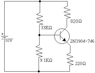
1) Assemble the following circuit:

2) Record the values of VB, VC, and VE.
3) Calculate IB, IC and b.
4) Replace the first transistor with a second.
5) Repeat steps 2 and 3.
6) Assemble the following circuit:

7) Repeat steps 2 and 3.
8) Replace the first transistor with a second.
9) Repeat steps 2 and 3.
10) Compare b and VBE to the theoretical values given in the text.
![]() Results
Results
A) Table 1: Values for Schematic 1
|
|
VB |
VC |
VE |
IB |
IC |
b |
|---|---|---|---|---|---|---|
|
Transistor 1 |
.59V |
5.4V |
0.0V |
34.6mA |
8.0mA |
231 |
|
Transistor 2 |
.60V |
5.8V |
0.0V |
34.5mA |
7.6mA |
220 |
B) Table 2: Values for Schematic 2
|
|
VB |
VC |
VE |
IB |
IC |
b |
|---|---|---|---|---|---|---|
|
Transistor 1 |
1.41V |
5.3V |
1.00V |
106mA |
5.73mA |
54.1 |
|
Transistor 2 |
1.68V |
5.4V |
1.01V |
68mA |
5.61mA |
82.5 |
C) Table 3: Values of VBE and b between experiments and given values.
Schematic #1 Schematic #2
|
|
Transistor 1 |
Transistor 2 |
Transistor 1 |
Transistor 2 |
Given |
|---|---|---|---|---|---|
|
VBE |
.59V |
.60V |
.41V |
.67V |
.65V |
|
b |
231 |
220 |
54.1 |
82.5 |
100 |
![]() Conclusions
Conclusions
From this experiment, one can see that in transistor biasing, the effects of component changes is greater on the second schematic than the first, when the transistors are swapped.
![]() Attachments
Attachments
A) Original Handout
B) Original Lab Data
C) Calculations