![]() Objective
Objective
The objective of this lab is to build and test and active 5th order low pass filter using a signal flow graph.
![]() Components Used
Components Used
1) PC with CircuitMaker® installed.
2) PC with MatLab®, Ocatve®, or SciLab® installed.
3) Oscilloscope #
4) Function Generator #
5) Analog Trainer #
6) Multimeter #
7) Various components from the EE-409 lab kit.
![]() Procedures
Procedures
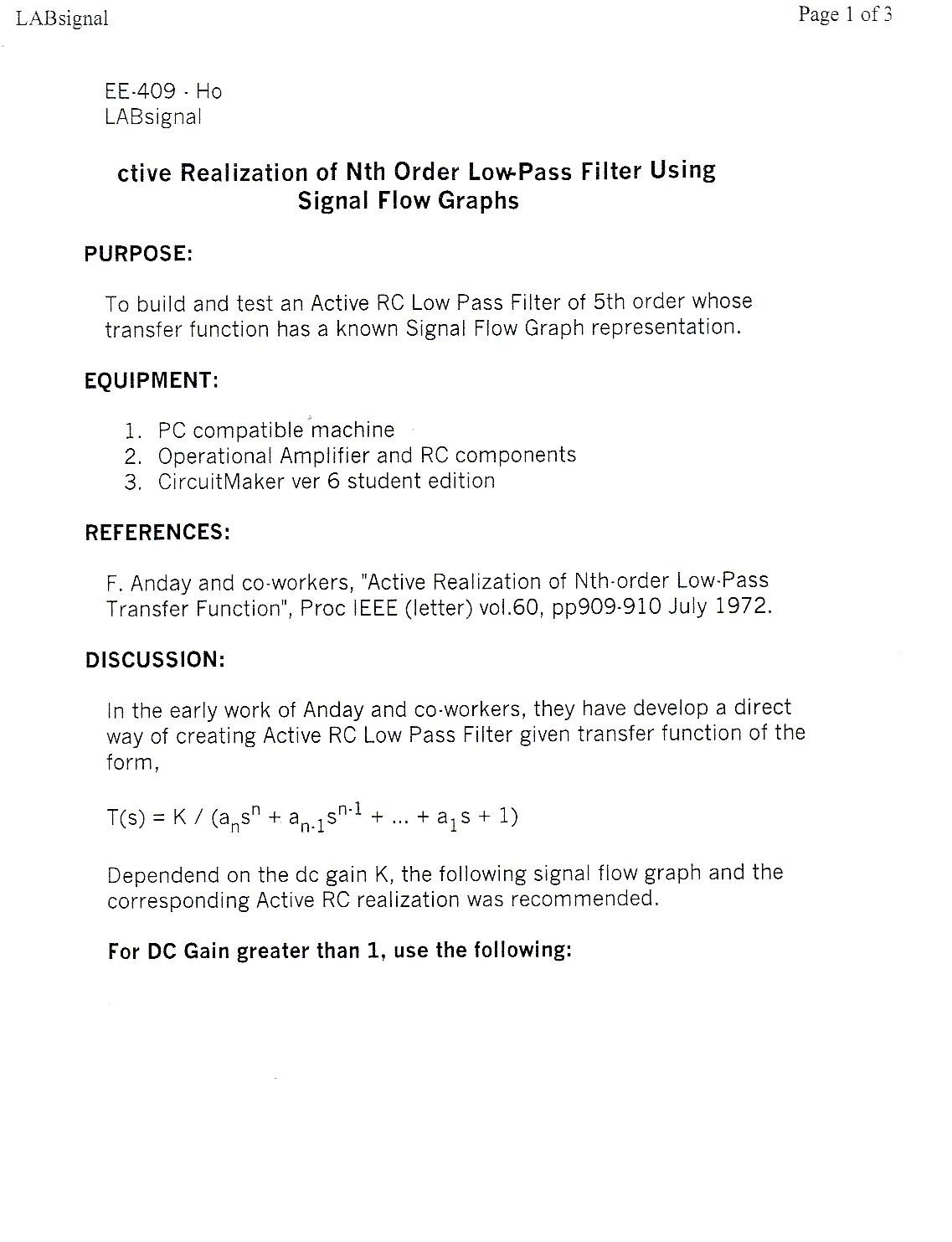
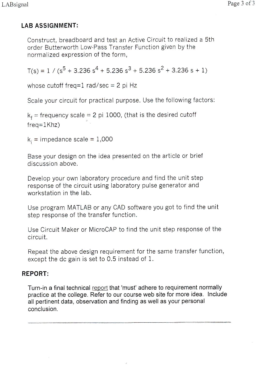
1) Design a 5th order active Butterworth low-pass filter with H(s) = 1/(s5 + 3.236*s4 + 5.236*s3 + 5.236s2 + 3.236s + 1)
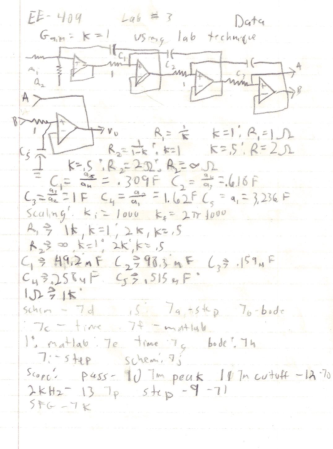
2) Scale the design so kf = 1KHz (2*p*1000) and ki = 1KW.
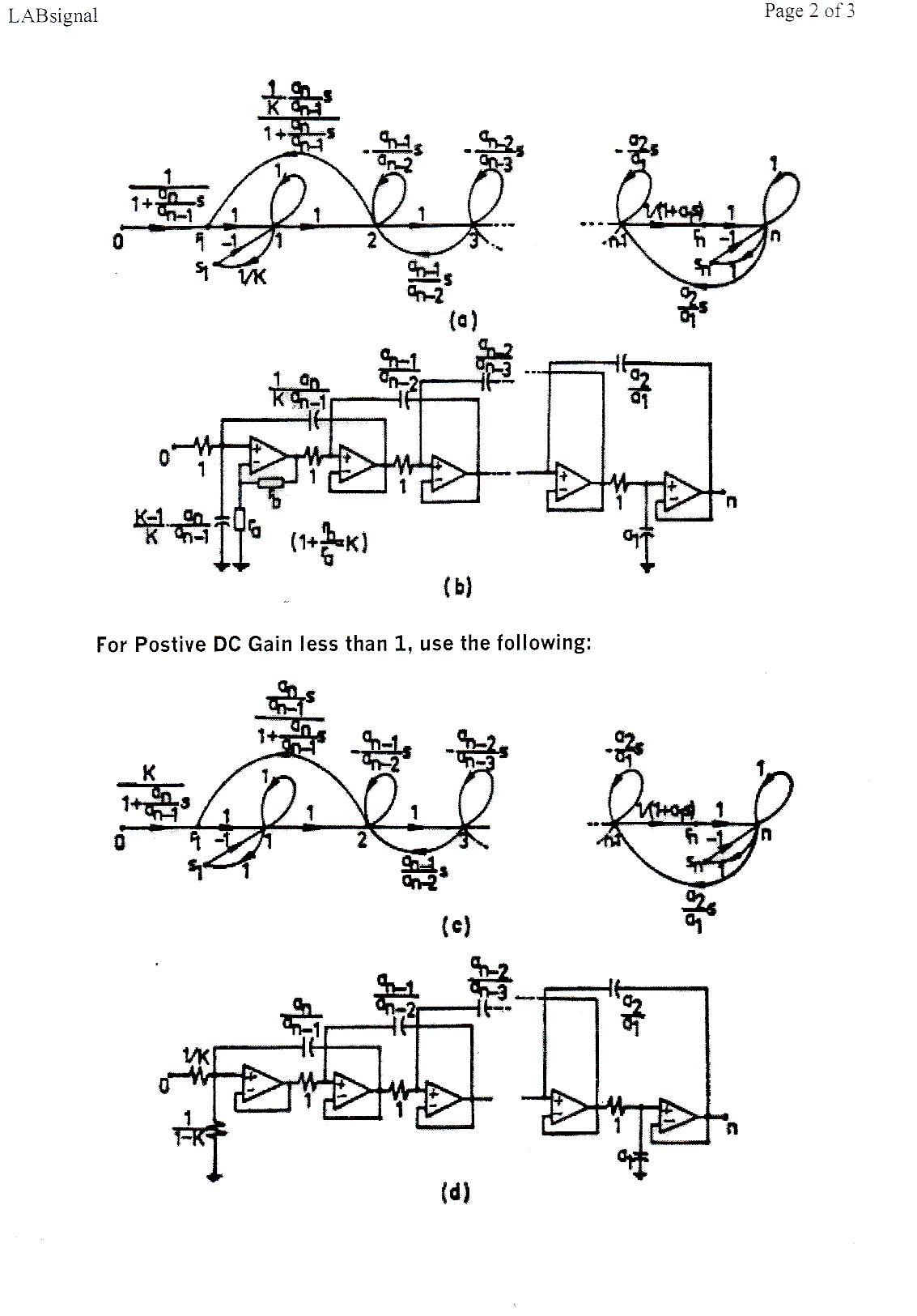
3) Illustrate the signal flow graph of the system.
4) Analytically find the system response to a unit step input.
5) Using MatLab®, or equivalent, find the output with a unit step input.
6) Using CircuitMaker®, verify the output with a unit step input.
7) Construct the circuit and demonstrate that the system responds properly to a step input.
8) Repeat steps 3 through 7 using a DC gain of .5.
![]() Lab Data / Results
Lab Data / Results
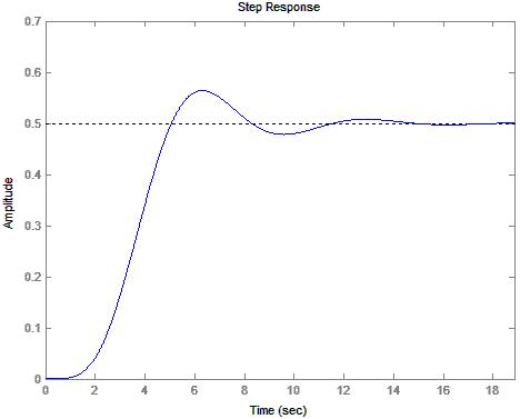
1) Diagram 1: Step Response Predicted by MatLab® for gain=.5
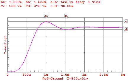
2) Diagram
2: Step Response Predicted by CircuitMaker® for gain=.5
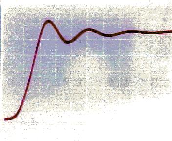
3) Diagram 3: Observed Step Response for gain=.5
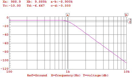
4) Diagram 4: Frequency Response Predicted by CircuitMaker®
5) Diagram
5: Signal Output with 1KHz input by CircuitMaker®
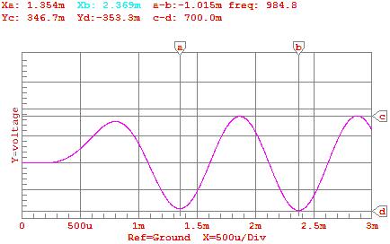
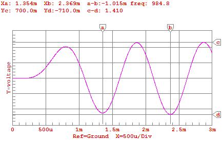
6) Diagram 6: Signal Output with Frequency <1KHz
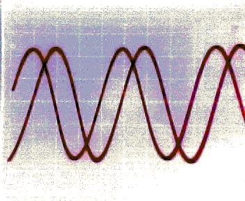
7) Diagram 7: Signal Flow Graph

8) Diagram
8: Signal Output with Frequency close to, but less than 1KHz
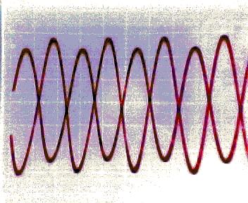
9) Diagram 9: Signal Output with F=1KHz
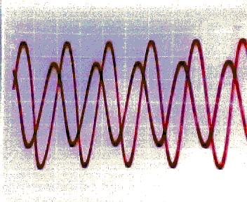
10) Diagram 10: Signal Output with F > 1KHz
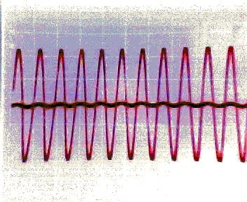
11) Diagram 11: Circuit with DC gain of .5

12) Diagram 12: Circuit with DC gain of 1

13) Diagram 13: Step Response Predicted by MatLab® for gain of 1
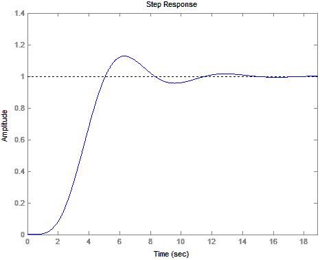
14) Diagram 14: Step Response Predicted by CircuitMaker® for gain of 1
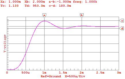
15) Diagram 15: Frequency Response Predicted by CircuitMaker®
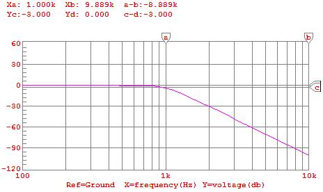
16) Diagram 16: Signal Output with 1KHz input by CircuitMaker®
![]() Conclusions
Conclusions
This lab has demonstrated the ability to realize a circuit using a signal flow graph. Although I did not attempt to find the transfer function using Mason's Gain Rule taught in Control I, a brief view of the signal flow graph shows that the original transfer function would be a solution. I was impressed on how accurately MatLab®, CircuitMaker, and the actual system were. The step responses are nearly identical. Also, the system shows the slight gain at frequencies near the cutoff frequency that is predicted by the step response. All captures of the actual system were taken using the DC gain of .5 and the vertical amplification for channel 2 (reference output) was twice that for channel 1 (system output). I did not employ a 1KW resistor between the output and ground. I felt that this is unnecessary since the design of operational amplifiers is based on voltage control and therefore will compensate naturally for mis-matched impedances. In order to construct capacitances of proper values for the realization of the circuit, I made the following simplifications: (note on syntax: || = parallel, -- = series) 49.2nF = 100nF -- 100nF; 98.3nF = 100nF; 159nF = 330nF – 330nF; 258nF = (470nF – 470nF) || (10nF || 10nF); 515nF = 470nF || 33nF. These simplifications did not significantly alter the frequency response. I was not able to calculate the sensitivity of the system due to the components and was therefore unable determine mathematically the change in frequency response as a result. It appeared to have shifted the cutoff frequency down by approximately 100Hz through experimentation. As mentioned, all data collected was done using K=.5 for simplicity. The practical demonstration will illustrate the system with K=1. One note is that the system is extremely sensitive to voltage variations between VCC and VDD and GND. In order to compensate for this, I used a slightly more complex setup that utilized a battery and series of electronic components and capacitors to compensate for this inherent instability. Among the key changes, I added a 330uF capacitor between VCC and VDD (+12V, -12V respectively), 330uF capacitor between VCC2 (+5V, used as a control signal to generate the step input) and GND, and 10uF capacitors between each of VCC and GND, and VDD and GND. The system appeared to stabilize considerably. To generate the step input, I used an additional OP amp in an non-inverting configuration with an input of 1V generated by a voltage divider from a known voltage source (+5V, VCC2). The signal was routed through a series of switches to generate the step and the output was sent to trigger an oscilloscope.
![]() Attachments
Attachments
