![]() Objective
Objective
EE - 401 / E01 Fall 2002
Introductory Communications Theory
Professor: Conner
Submitted By:
Andrew Buettner
Lab #2: Amplitude Modulation
Table Of Contents
1) Cover Page 1
2) Table of Contents 2
3) Objective 4
4) Components Used 4
5) Procedures 4
6)
Lab Data / Results 5
1) Diagram 1 5
2) Diagram 2 5
3) Diagram 3 6
4) Diagram 4 6
5) Diagram 5 7
6) Diagram 6 7
7) Diagram 7 8
8) Diagram 8 8
9) Diagram 9 9
10) Diagram 10 9
11) Diagram 11 10
12) Diagram 12 10
13) Diagram 13 11
14) Diagram 14 11
15) Diagram 15 12
16) Diagram 16 12
17) Diagram 17 13
18) Diagram 18 13
19) Diagram 19 14
20) Diagram 20 14
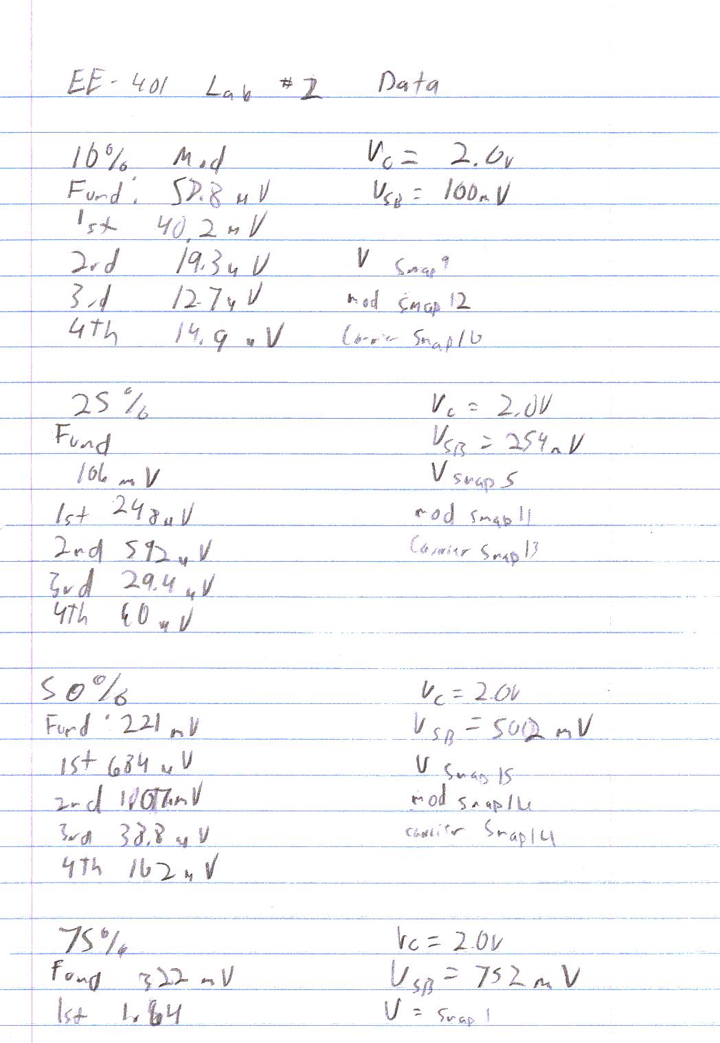
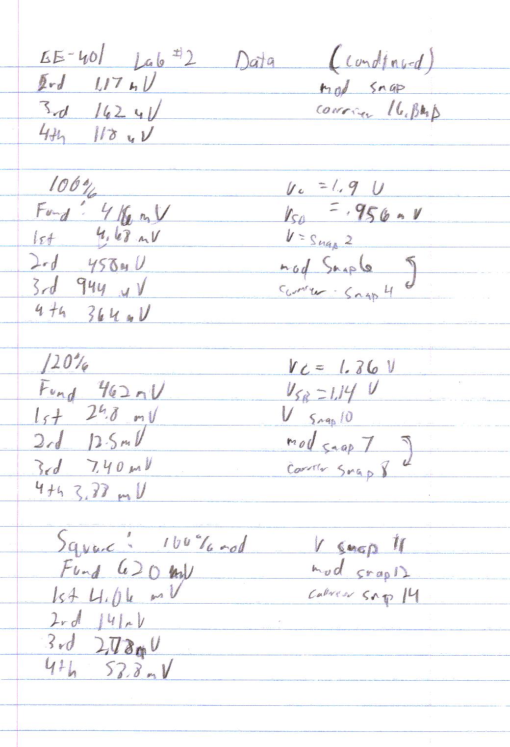
21) Table 1 15
22) Diagram 21 15
23) Diagram 22 16
24) Table 2 16
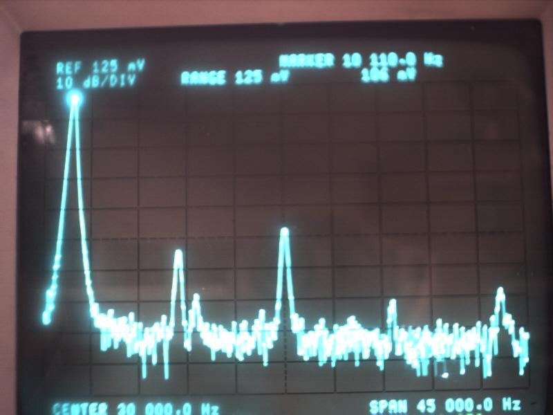
25) Diagram 23 17
26) Table 3 17
27) Diagram 24 18
28) Diagram 25 18
7) Answers to Lab Questions 19
8) Conclusions 19
8) Attachments 20
![]() Objective
Objective
The objective of this lab is to gain in understanding of the significance of modulation bandwidth and index in AM or DSB-FC modulation by generating several different modulation patterns with several different modulation indexes and then calculated the amount of noise that is introduced into each signal.
![]() Components Used
Components Used
1) AF Spectrum Analyzer #1663
2) RF Spectrum Analyzer #1939
3) Function Generator #1510
4) Modulating Function Generator #1511
5) Various components from the EE-301/401 Lab Kit
6) Oscilloscope #1663
7) Trainer #50715653
![]() Procedures
Procedures
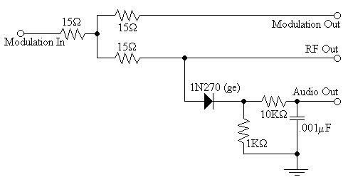
1) Assemble
the following circuit:

2) Apply a DSB-FC signal to the input.
3) Set the AM signal to have a FC of 1MHz and FM of 10KHz.
4) Set the output to 10Vp-p.
5) Connect the oscilloscope channel one to the RF output.
6) Connect the oscilloscope channel two to the demodulated output.
7) Modulate the signal with a modulation index of 10%
8) Show the output waveform and spectrum.
9) Calculate the total harmonic distortion that appears at the output.
10) Repeat steps 7 - 9 using a modulation index of 25%
11) Repeat steps 7 - 9 using a modulation index of 50%
12) Repeat steps 7 - 9 using a modulation index of 75%
13) Repeat steps 7 - 9 using a modulation index of 100%
14) Repeat steps 7 - 9 using a modulation index of 120%
15) Change the modulation signal to a 50% duty cycle , 5KHz square wave with a modulation index of 100%.
16) Sketch the input and output waveforms.
17) Calculate the expected size of the spectral lines.
18) Compare the size of the spectral lines with the observed ones.
19) Repeat steps 15 - 18 using a triangle wave.
![]() Lab Data / Results
Lab Data / Results
1) Diagram 1: Schematic (Enlarged View)
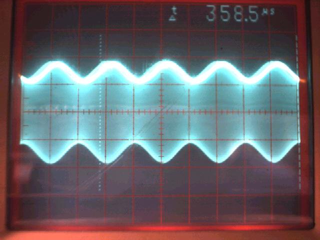
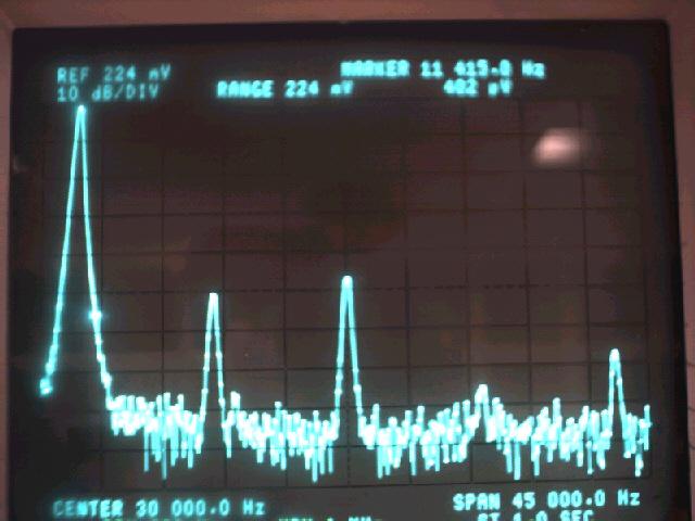
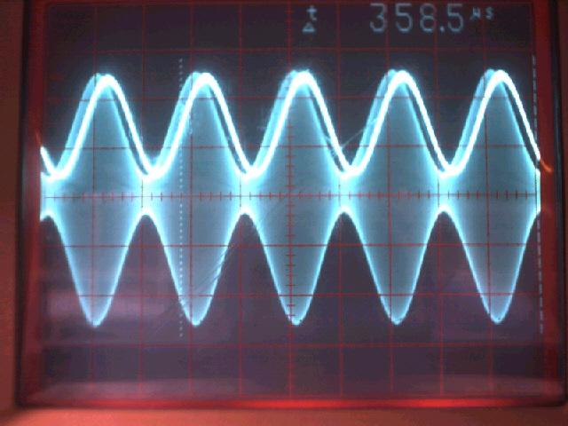
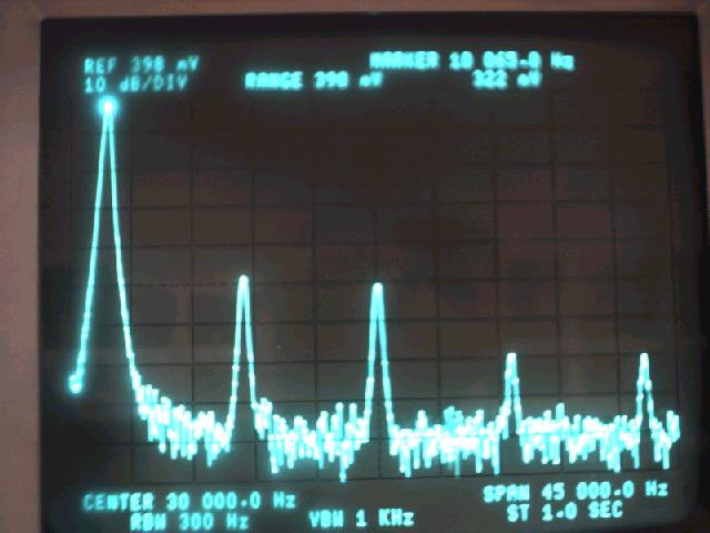
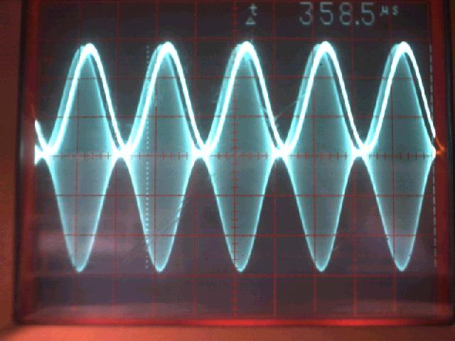
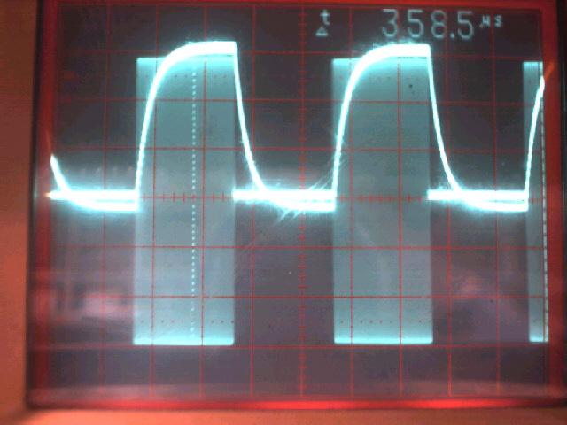
2) Diagram 2: Voltage / Time view of 10% Modulation:
3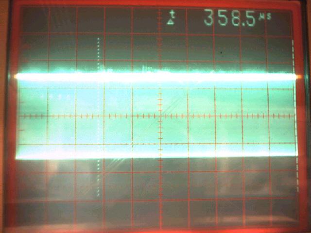
) Diagram
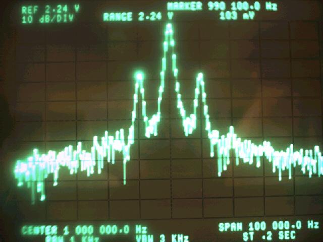
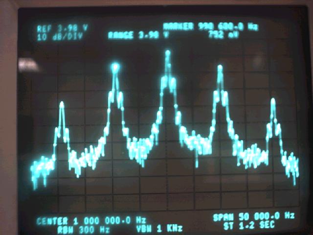
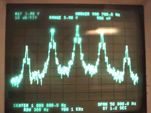
3: Voltage / Frequency View of 10% Modulation:
4) Diagram
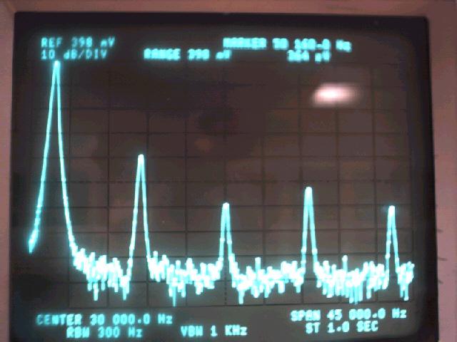
4: Voltage / Frequency View of Demodulated Output:

5) Diagram
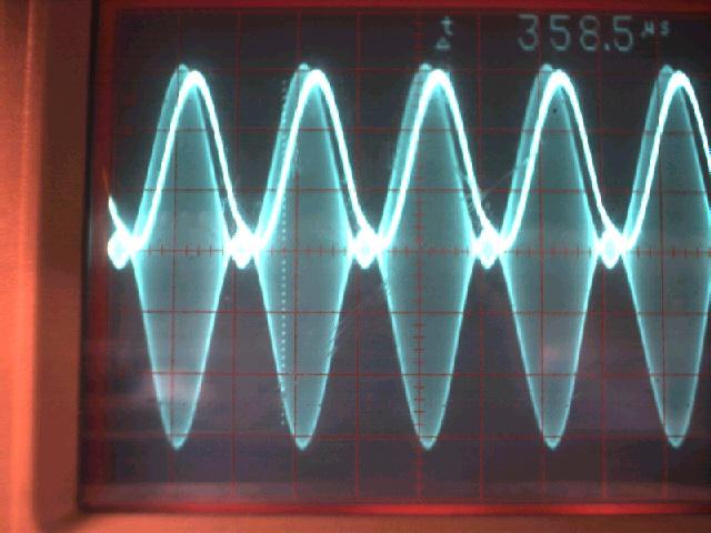
5: Voltage / Time View of 25% Modulation:
6) Diagram
6: Voltage / Frequency View of 25% Modulation:
7) Diagram
7: Voltage / Frequency View of Demodulated Output:
8) Diagram
8: Voltage / Time View of 50% Modulation:
9) Diagram
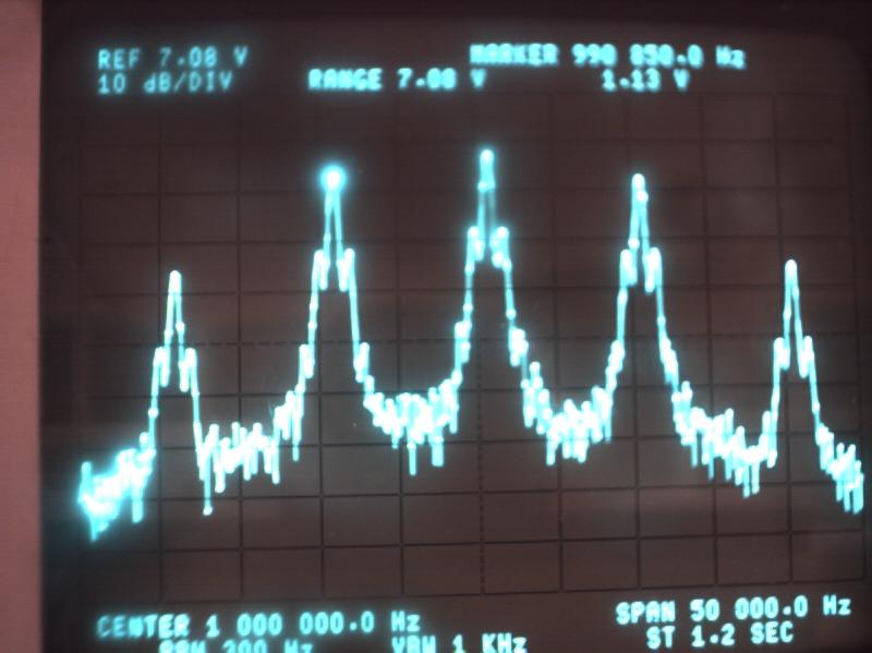
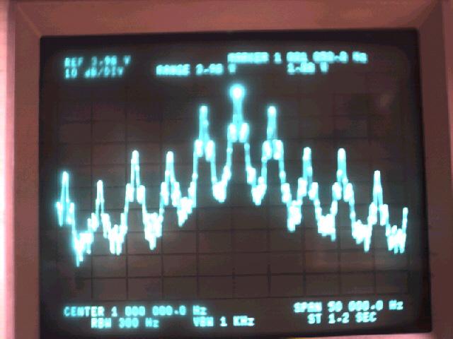
9: Voltage / Frequency View of 50% Modulation:
10) Diagram
10: Voltage / Frequency View of Demodulated Output:
11) Diagram
11: Voltage / Time View of 75% Modulation:
12) Diagram
12: Voltage / Frequency of 75% Modulation:
13) Diagram
13: Voltage / Frequency View of Demodulated Output:
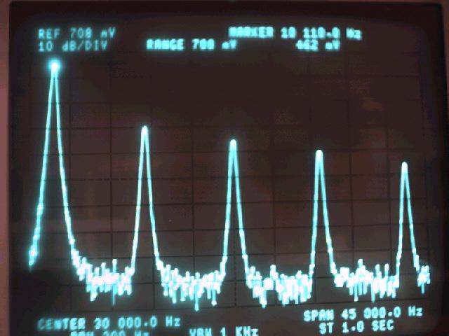
14) Diagram
14: Voltage / Time View of 100% Modulation:
15) Diagram
15: Voltage / Frequency View of 100% Modulation:
16) Diagram
16: Voltage / Frequency View of Demodulated Output:
17) Diagram
17: Voltage / Time View of 120% Modulation:
18) Diagram
18: Voltage / Frequency View of 120% Modulation:
19) Diagram
19: Voltage / Frequency View of Demodulated Output:
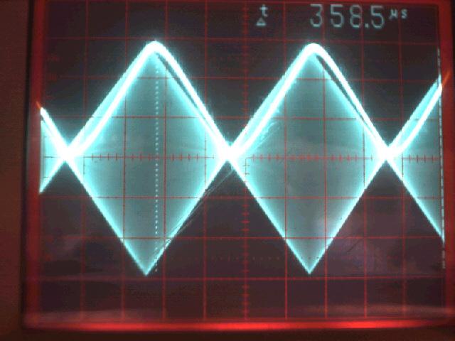
20) Diagram
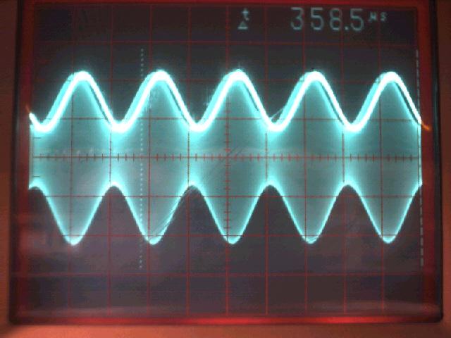
20: Frequency / Time View of Square Wave Modulation:
21) Table
1: Harmonic Distortions of Various Modulation Indices:
|
|
Fundamental: |
1st |
2nd |
3rd |
4th |
Total: |
%Of Total: |
|---|---|---|---|---|---|---|---|
|
10%: |
58.8mV |
40.2mV |
19.3mV |
12.7mV |
14.9mV |
87.1mV |
75.2% |
|
25%: |
106mV |
248mV |
592mV |
29.4mV |
60.0mV |
929.4mV |
46.7% |
|
50%: |
221mV |
684mV |
1.07mV |
38.8mV |
102mV |
1.8948mV |
.850% |
|
75%: |
322mV |
1.04mV |
1.17mV |
162mV |
118mV |
2.49mV |
.767% |
|
100%: |
416mV |
4.68mV |
458mV |
944mV |
364mV |
6.446mV |
1.53% |
|
120%: |
462mV |
4.06mV |
141mV |
2.78mV |
58.8mV |
7.0398mV |
1.50% |
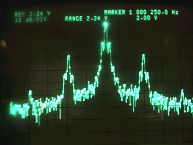
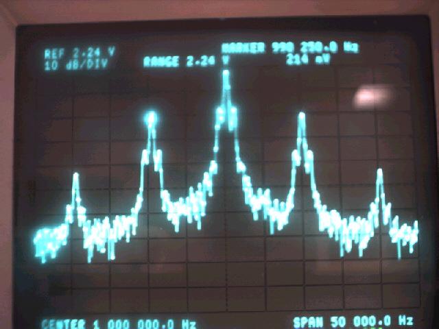
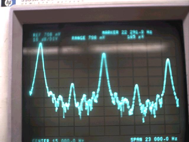
22) Diagram 21: Voltage / Frequency View of Square Wave Modulation:
23) Diagram 22: Voltage / Frequency View of Demodulated Output:
24) Table 2: Harmonic Distortion of Demodulated Square Wave:
|
|
Fundamental: |
1st |
2nd |
3rd |
4th |
Total: |
% 0f Total: |
|---|---|---|---|---|---|---|---|
|
Expected: |
620mV |
207mV |
0 |
124mV |
0 |
0 |
0 |
|
Observed: |
620mV |
406mV |
141mV |
278mV |
58.8mV |
0 |
0 |
|
Total: |
0 |
199mV |
141mV |
154mV |
58.8mV |
353.2mV |
0 |
|
% Of Total |
0 |
32.9% |
100% |
35.6% |
100% |
0 |
36.3% |
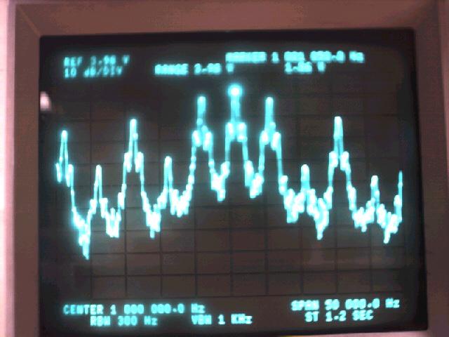
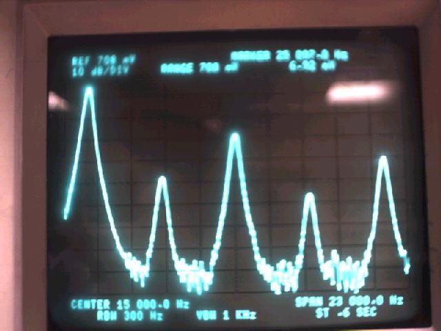
25) Diagram 23: Frequency / Voltage View of Triangle Wave Modulation:
26) Table 3: Harmonic Distortion of Triangle Wave:
|
|
Fundamental: |
1st |
2nd |
3rd |
4th |
Total: |
% 0f Total: |
|---|---|---|---|---|---|---|---|
|
Expected: |
406mV |
0 |
45.1mV |
0 |
16.2mV |
0 |
0 |
|
Observed: |
406mV |
3.06mV |
28.4mV |
1.09mV |
6.92mV |
0 |
0 |
|
Total: |
0 |
3.06mV |
16.7mV |
1.09mV |
9.28mV |
30.1mV |
0 |
|
% Of Total: |
0 |
100% |
37.0% |
100% |
57.3% |
0 |
6.91% |
27) Diagram 24: Voltage / Time View of Triangle Wave Modulation:
28) Diagram
25: Voltage / Frequency View of Demodulated Output:
![]() Answers
to Lab Questions
Answers
to Lab Questions
1) Q: Why was the power splitter used, and how does it operate?
A: It was used to divide the power between the two theoretical 50W outputs directly while still providing a 50W input to maintain maximum power transfer and keeping the SWR as close as possible to a theoretical 1. Otherwise, the Vx or Ix could become high from either a j or Z not being equal to 50W and damage the internal components. Note: Having an SWR not 1:1 also causes a situation called ground current which can cause RF burns. See attachments for more information.
2) Q: As the modulation percentage increased, what happened to the amount of harmonic distortion, why did this happen?
A: The distortion dropped off significantly because there was more of a reference signal and the diode was set into it's saturation point.
3) Q: Explain why the demodulated square wave and triangle wave had more distortion to them than the sine wave.
A: The waves had more distortion for multiple reason. The most significant being, that they require infinite bandwidth. Also, the signals could be processed differently because the signal nature and reactance of the modulator. Lastly there was no definitive way to ensure that the modulation index was perfectly 100%, it is possible that the modulation index was slightly higher than that and caused a significant amount of distortion in the signal, especially at overtones.
4) Q: What is the bandwidth required to send the following signal VIA DSB-SC: cos(2000pt) + cos(4000pt) + cos(6000pt)?
A: 12KHz
![]() Conclusions
Conclusions
This lab has demonstrated some of the basic principles of DSB-FC modulation. Significant problems in the lab involved the fact that there wasn't a function generator capable of putting out a signal with enough voltage to obtain the required voltage. As a result, all specified voltages were divided by two during the actual experiment. Also, the generators were not designed for 50W loads, instead they were Hi-Z outputs (S100KW). As a result, the 50W resistor from the diode input to ground was removed during the experiment. Also, calculations are not compensated for harmonic distortions inherent to the function generators. That was somewhat discussed in the explanation of question 3. Other than that there were no other difficulties with this lab.
![]() Attachments
Attachments
Original lab handout
Original lab data
Calculations