![]() Objective
Objective
The objective of this lab is to create an amplifier with multiple inverting, and non inverting inputs. This will be accomplished by using a single 741 style op-amp. Then measurements will be bade on the simulated circuit and compared to expected, calculate values.
![]() Components Used
Components Used
1) PC with CircuitMaker® installer
![]() Procedures
Procedures
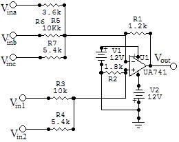
1) Design a multi-input amplifier / summer that follows the following equation: Vo = V1 + 2V2 - 3Va - Vb - 2Vc
2) Simulate the circuit using all 1V inputs.
3) Repeat step 2 using a 1Vp-p sine wave at 1KHz
4) Repeat step 2 using a 1Vp-p AM wave form with a carrier frequency of 10KHz and modulation of 1KHz.
5) Repeat step 2 using a 1Vp-p FM wave with the same characteristics as the AM wave.
![]() Lab
Data / Results
Lab
Data / Results
1) Diagram 1: Summer / Amplifier Schematic

2) Table 1: Results from DC test
|
DC Voltage Output: |
-107.2mV |
3) Diagram 2: Result from sinewave test

4) Diagram 3: Results from AM test

5) Diagram 4: Results from FM test

![]() Answers to Lab Questions
Answers to Lab Questions
1) Q: Derive Phil Vrbancic's theorem.
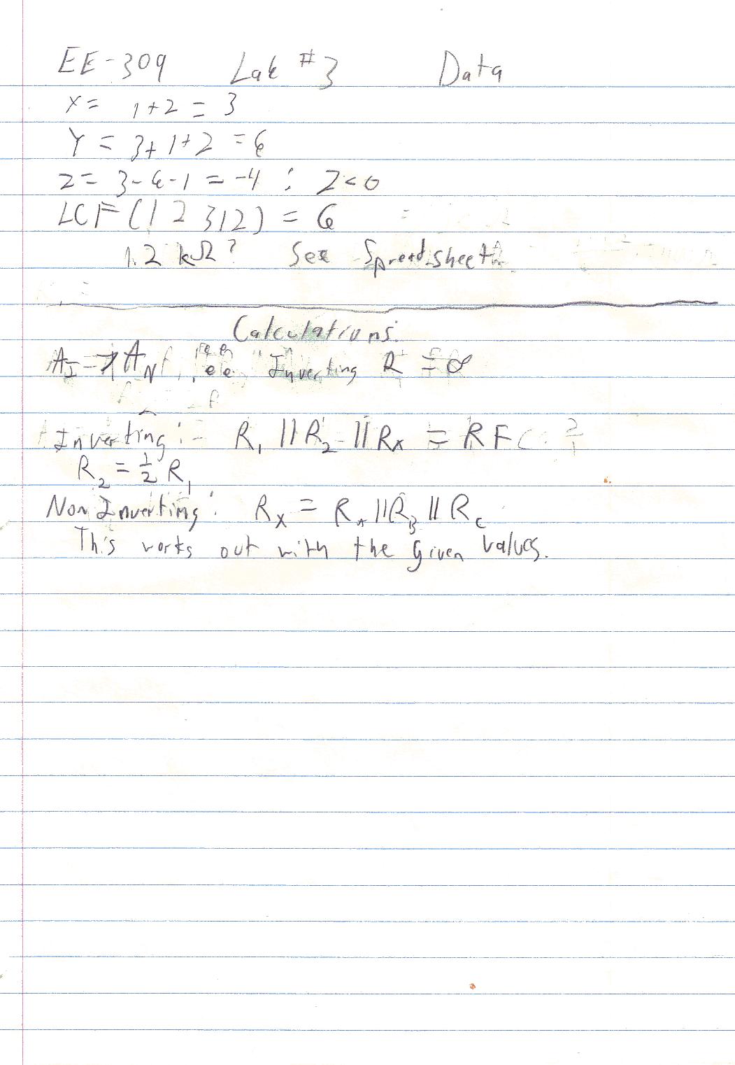
A: See Attachments
![]() Conclusions
Conclusions
This lab has demonstrated the basics of a summer / amplifier. My answer to the post lab question may not be completely correct because I mostly guessed as to the Rx relationship. However, the system makes sense when considering the principle of inverting, and non-inverting configurations.
![]() Attachments
Attachments
